
PV inspection
PV Inspection Lasers: Configure the Excitation Source
Lumexis supplies fiber-coupled laser sources for photovoltaic photoluminescence inspection, with wavelength, sample-plane irradiance, uniformity, camera response, filtering, and production cycle time reviewed as one system.
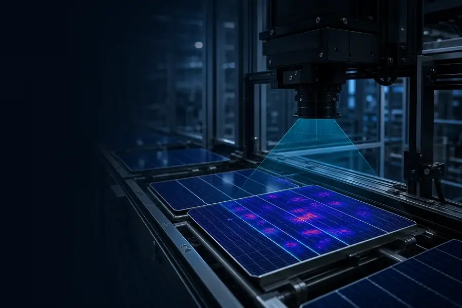
Lumexis supplies fiber-coupled lasers for PV inspection equipment that uses optical excitation to image photoluminescence from crystalline-silicon wafers, cells or modules. Our 808 nm source family is the primary starting point for this application; 915 nm custom configurations and published 976 nm models can be evaluated where absorption depth, filtering and system geometry justify a different wavelength.
The laser is one part of the measurement chain. Useful defect contrast depends on uniform irradiance at the sample, camera sensitivity near the silicon emission band, rejection of reflected excitation, sample temperature, electrical operating condition and image calibration. We therefore configure the source around the inspection result—not around optical watts alone.
Choose the solution by inspection stage
| Inspection stage | What PL imaging can contribute | Source-design priority |
|---|---|---|
| Silicon material and wafer characterization | Spatial variation associated with carrier lifetime and recombination behavior | Stable, homogeneous excitation and calibrated intensity |
| Cell-process development | Comparison of passivation, firing and contact-process outcomes | Repeatable sample condition and controlled injection level |
| Cell production inspection | Fast imaging of non-uniform regions, interruptions and inactive areas | Cycle time, full-area uniformity and automated handling |
| Module laboratory analysis | Contactless optical excitation where electrical injection is inconvenient | Larger illuminated field, power scaling and stray-light control |
| R&D measurement platforms | Injection-dependent or modulated PL experiments | Power control, modulation, camera synchronization and traceable geometry |
Quick match: use 808 nm as the default discussion for silicon PL imaging when a proven excitation architecture and straightforward separation from the longer-wavelength emission are priorities. Evaluate 915 or 976 nm only after checking absorption, required irradiance, filter margin and the detector’s spectral response.
What photoluminescence imaging measures
When silicon absorbs photons with energy above its bandgap, electron-hole pairs are generated. A small fraction of the subsequent recombination produces near-infrared light. A sensitive camera maps that weak luminescence across the wafer or cell.
Dark or bright variations can correlate with changes in local recombination, material quality, voltage or electrical condition. Depending on the process stage and analysis method, PL images may reveal or help classify:
- recombination-active regions;
- cracks or interrupted regions that alter carrier distribution;
- non-uniform passivation or processing;
- inactive or electrically isolated areas;
- spatial variation used in carrier-lifetime or implied-voltage analysis.
An image is not a diagnosis by itself. The same visual pattern can have more than one cause, and quantitative interpretation requires controlled excitation, sample condition, calibration and an appropriate physical model.
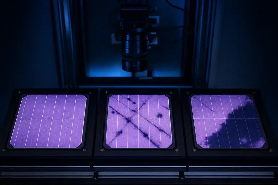
Measurement response
Interpret the optical response in application context
Conceptual photovoltaic photoluminescence maps showing uniform, cracked and inactive regions
PL, EL and ordinary visual inspection are different tools
Photoluminescence imaging
PL uses external optical excitation. It can inspect non-contacted wafers or cells and can be configured for research or production workflows. The laser source, homogenizer, camera and filters form the central optical chain.
Electroluminescence imaging
EL injects electrical current into a contacted cell or module. It does not require an optical excitation laser, but it needs electrical access and controlled current injection. EL and PL may show related features under different operating conditions; they are not interchangeable measurements.
Reflectance and visible inspection
Conventional cameras detect surface appearance, print alignment, contamination and geometric defects. They do not directly measure the weak band-to-band luminescence used in silicon PL. A production tool may combine these methods, but each channel needs its own illumination and calibration.
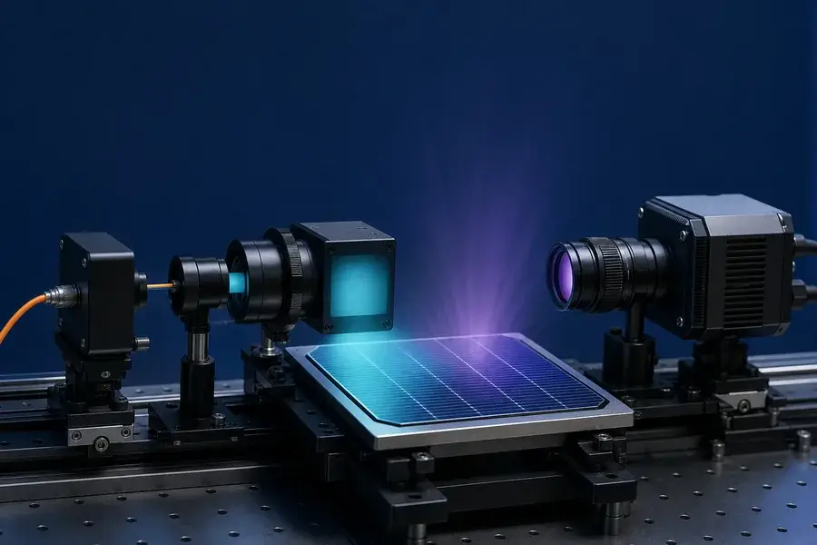
The PV photoluminescence optical chain
A practical station typically includes:
- Fiber-coupled excitation source — provides a controlled 808, 915 or 976 nm wavelength and optical power.
- Delivery fiber and termination — routes power away from the inspection head and into the illumination optics.
- Collimation and homogenization — converts the fiber output into a broad field with defined spatial uniformity.
- Silicon sample and operating fixture — controls position, temperature and, where needed, electrical loading.
- Collection lens and rejection filter — transmits the luminescence band while suppressing reflected excitation and ambient light.
- Sensitive camera — captures the weak near-infrared signal with an exposure compatible with the line cycle.
- Calibration and analysis — corrects illumination non-uniformity, camera response and other systematic effects before classification or parameter extraction.
System architecture
Review the complete optical and measurement chain
PV photoluminescence optical chain with fiber laser, homogenizer, solar cell, filter and camera
Wavelength selection: 808 vs 915 vs 976 nm
All three wavelengths are shorter than the silicon band-edge emission region and can generate carriers in crystalline silicon. They are not equivalent in an imaging system.
808 nm: the primary starting point
808 nm fiber-coupled sources are widely used in published silicon PL imaging setups. The wavelength provides strong silicon absorption and leaves useful spectral distance between reflected excitation and the longer-wavelength luminescence signal. That separation supports a long-pass filtering approach in suitable systems.
Use 808 nm when:
- established silicon-cell PL architectures are the reference;
- high absorbed excitation near the illuminated surface is desired;
- a long-pass filter can separate the luminescence band from excitation;
- published Lumexis power classes from 25 to 400 W fit the optical budget.
915 nm: a custom evaluation option
Moving toward 915 nm changes the absorption profile and the relationship between excitation and emission filtering. It may be useful when an equipment team has already validated this wavelength in its material stack, camera and optical design. Lumexis should confirm availability, wavelength tolerance, power class and fiber interface for each program; no standard 915 nm model is listed in the current public model set.
976 nm: closer to the band edge
At 976 nm, absorption in silicon is generally weaker and extends deeper than at 808 nm. That can be relevant to bulk-sensitive inspection concepts, but it also changes the required optical power density and reduces the spectral margin available for blocking reflected excitation while passing the PL signal. Filter edge quality, camera sensitivity and stray-light control become especially important.
Use 976 nm only after a system trial confirms that the deeper excitation profile produces useful information at an acceptable exposure and thermal load.
Irradiance and uniformity—not total watts—drive the measurement
Laser output power is distributed by the illumination optics over an area. The useful engineering quantity at the sample is irradiance:
E = Psample / A
where (Psample) is optical power reaching the illuminated sample and (A) is illuminated area. For a full cell, that area can be much larger than a laboratory spot, so the same source power produces a much lower irradiance.
The average value is only the beginning. A bright center and dark corners create a false spatial pattern that can be mistaken for material variation. Specify:
- illuminated width and length;
- average irradiance at the sample;
- peak-to-average or maximum-to-minimum uniformity metric;
- edge roll-off and excluded border;
- temporal stability during one exposure and across a production shift;
- repeatability after source warm-up and maintenance.
Flat-field correction can compensate for part of a stable illumination pattern, but it cannot recover signal from severely under-illuminated regions or correct a pattern that changes with temperature, fiber movement or optical contamination.
Camera and filter matching
Silicon band-edge luminescence is weak and lies near the long-wavelength limit of conventional silicon detectors. Cooled silicon cameras or InGaAs cameras may be used depending on sensitivity, exposure, resolution and cost targets.
The detector decision influences the whole source specification:
- Spectral response: confirm sensitivity across the intended PL collection band, not just a nominal camera range.
- Noise: dark current, read noise and fixed-pattern noise matter when the signal is weak.
- Exposure and frame rate: production cycle time may require more excitation, a faster lens or a more sensitive camera.
- Pixel sampling: small defects require enough spatial sampling after the complete lens and working-distance geometry is included.
- Cooling and stabilization: camera temperature affects noise and calibration stability.
A long-pass or band-selection filter is normally used to reject reflected excitation. The filter must provide sufficient blocking at the laser wavelength while maintaining transmission in the useful PL band. Leaks, off-axis behavior and scattered light from mechanical surfaces can overwhelm the desired signal even when the nominal filter curve looks acceptable.
Source parameters to specify
Output power at a defined plane
State whether power is measured at the module, fiber termination, homogenizer output or sample. Include the intended operating point and modulation condition. This prevents an optical-loss assumption from becoming a system-level performance gap.
Wavelength and spectral width
The wavelength must remain inside the intended excitation region and outside the filter’s collection band over temperature and operating current. Spectral width matters because the rejection filter must block the full source spectrum, not only its center wavelength.
Fiber core and numerical aperture
Core diameter and numerical aperture determine how the output couples into a collimator, beam expander or homogenizer. A larger core can simplify power handling but changes étendue and the minimum achievable beam properties. Select the fiber and illumination optics together.
Power stability and modulation
For quantitative or lock-in methods, define modulation frequency, rise/fall behavior and synchronization with the camera. For steady-state imaging, include short-term noise and long-term drift at the chosen thermal condition.
Thermal and electrical integration
High optical power requires a controlled heat-removal path and an appropriate driver. The equipment should monitor relevant temperatures and prevent operation outside the agreed envelope. Thermal drift can change optical output and can also heat the sample, altering the measurement being made.
Fiber safety and contamination control
Near-infrared output is not visible to the operator. The beam path should be enclosed, access controlled and reviewed under the integrator’s laser risk assessment. Fiber end faces and connectors require clean handling; contamination at high power can create localized heating and permanent damage.
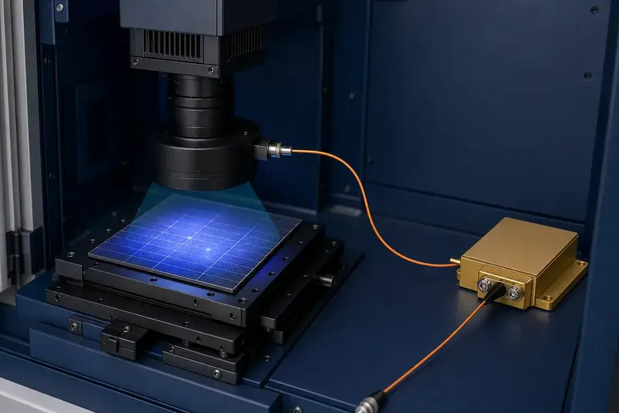
System architecture
Review the complete optical and measurement chain
808 nm fiber-coupled laser integrated into a photovoltaic photoluminescence inspection cabinet
Lumexis source families for PV inspection evaluation
Published 808 nm models
| Model | Published optical power | Evaluation role |
|---|---|---|
| 808-LXGX0025 | 25 W | Laboratory or smaller-area excitation trials |
| 808-LXGX0050 | 50 W | Cell-level PL development and moderate optical-loss budgets |
| 808-LXGX0150 | 150 W | Larger fields, shorter exposures or production-tool development |
| 808-LXGX0400 | 400 W | Specialized high-throughput systems with engineered homogenization and cooling |
Published 976 nm models
| Model | Published optical power | Evaluation role |
|---|---|---|
| 976-LXGX0120 | 120 W | Initial near-band-edge excitation trials |
| 976-LXGX0140 | 140 W | Alternative power and package evaluation |
| 976-LXGX0260 | 260 W | Larger-area or higher-loss optical systems |
| 976-LXGX0280 | 280 W | High-throughput development with confirmed filter margin |
| 976-LXGX0750 | 750 W | Specialized high-power platforms with dedicated thermal design |
These tables identify published power classes, not guaranteed sample irradiance or inspection speed. Fiber geometry, connector, spectral characteristics, drive conditions and package must be confirmed against the current controlled specification. A 915 nm requirement should be treated as a custom configuration review.
Building an inline PV inspection station
1. Define the sample and question
Specify whether the tool inspects ingots, bricks, wafers, cells or modules. List the process defects or material variations that matter and whether the output is qualitative classification or a calibrated parameter map.
2. Set the cycle-time and image-quality target
Provide transport speed, handling time, exposure allowance, field of view and minimum feature size. These establish camera sampling and the required photon budget.
3. Select wavelength with the detector and filter
Do not choose the source separately. Test excitation wavelength, filter set and camera on representative samples. Confirm that reflected excitation remains below the camera’s usable background level across the full field.
4. Design the homogenizer around the sample area
Model or measure collimator acceptance, diffuser or microlens-array loss, uniformity and edge roll-off. Include the distance from homogenizer to sample and sensitivity to alignment.
5. Close the optical and thermal budgets
Calculate required power at the sample and work backward through losses. Evaluate sample heating at the intended irradiance and duty cycle. Design the laser cooling system for steady operation, not only a short laboratory exposure.
6. Calibrate and validate
Collect dark frames, flat fields and reference-sample data. Test repeatability after warm-up, fiber movement, optical cleaning and part-position variation. Quantitative PL methods require a documented calibration procedure and controlled sample conditions.
Information to send Lumexis
For a source recommendation, send:
- silicon material and inspection stage;
- sample dimensions and illuminated area;
- desired wavelength or current reference setup;
- required irradiance and uniformity metric at the sample;
- camera type, lens, filter and exposure time;
- operating mode: continuous, pulsed or modulated;
- production cycle time and annual throughput;
- fiber core, numerical aperture, connector and length preferences;
- source mounting envelope, cooling method and ambient range;
- prototype quantity, validation schedule and expected annual volume.
Frequently asked questions
Why is 808 nm commonly used for silicon PL imaging?
It is absorbed by crystalline silicon, is available in practical fiber-coupled power classes and can be separated from the longer-wavelength silicon luminescence with an appropriate optical filter. Published research includes 808 and 810 nm excitation systems for silicon-cell imaging.
Can 976 nm replace 808 nm without changing the system?
No. Silicon absorption depth, required irradiance and filter separation change with wavelength. The homogenizer, camera filter, stray-light control and exposure may all require revalidation.
Is PL inspection suitable for uncontacted wafers?
Yes. Optical excitation is one reason PL is valuable before a sample has finished electrical contacts. Interpretation still depends on the material state and the selected analysis method.
What is the difference between a dark area and a crack?
A dark PL region indicates reduced detected luminescence under the measurement condition. Cracks, recombination, electrical isolation, shading or non-uniform excitation can produce different dark patterns. Classification should be validated against known samples and complementary measurements.
How much laser power is required for a full solar cell?
There is no universal wattage. Required power follows the illuminated area, target irradiance, homogenizer loss, exposure time, camera sensitivity and wavelength-dependent absorption. Define power at the sample plane and include a measured uniformity specification.
Can PL imaging operate in normal factory light?
It can be engineered for an enclosed production environment using optical filters, shielding and controlled exposure. Uncontrolled ambient light adds background and variability, so enclosure design remains important.
Configure the excitation source as part of the measurement
Share your sample, image target, camera, filter and cycle time. Lumexis will help compare 808, 915 and 976 nm options, establish a realistic sample-plane power budget, and define the fiber and thermal interface for prototype validation and OEM production.
Lumexis — precision laser sources, engineered for the real world.
Technical references
- NREL: Temperature-Dependent Photoluminescence Imaging of a Multicrystalline Silicon Solar Cell
- Fraunhofer ISE: Photoluminescence Imaging as a Spatially Resolved, Contactless Method
- Chinese Physics B: Fiber-Coupled 808 nm Excitation for Silicon Cell PL Imaging
- Progress in Photovoltaics: Photoluminescence Imaging of Silicon Modules
- J-STAGE: Photoluminescence Imaging for Semiconductor Substrates